Technical Support

Early involve in customer design and project communication
Communicaion how to choose material( According signal speed, loss and so on)
Determine what kind of PCB technology will be used, Such as HDI,Rigid-flex,Back drill, embeded coin and on on)
Help customer to build stackup, Impedance simulation, layout suggestion
Provide design rules for customer reference to improve Yield in process

Project start or in-process technical exchange and support
1. Technical DFM communication before product put into production. Confirm it is fine to production or where need to ajust to meet production. 2. Monitor the online yield status during the anufacturing process and maintain communication with customers.

Technical communication and support afer delivery
Technical support during SMT process
Technical communication in the process of product debugging
Technical communication in qualification of product reliablity
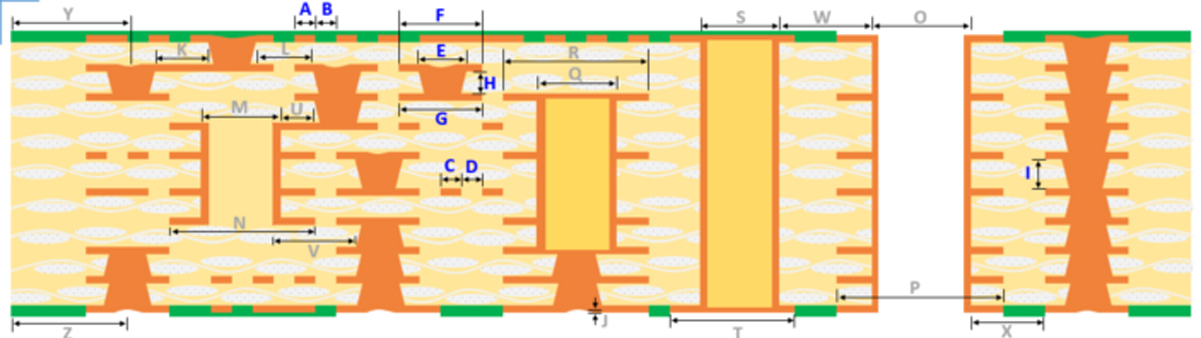
| Design rules of HDI | |||||
|---|---|---|---|---|---|
 |
|||||
| Symbol | Description | Standard | Advanced | ||
| A | Minimum line width on outer layer | 50 | 40 | ||
| B | Minimum line spacing on outer layer | 50 | 40 | ||
| C | Minimum line width on inner layer | 50 | 40 | ||
| D | Minimum line spacing on inner layer | 50 | 40 | ||
| E | Minimum blind via hole size | 75 | 75 | ||
| F | Minimum blind via capture pad size | E + 120 | E + 80 | ||
| G | Minimum blind via land pad size | E + 120 | E + 80 | ||
| H | Laminated prepreg thickness | E * 0.5 ~ E * 0.8 | E * 0.5 ~ E * 1 | ||
| I | Anylayer core thickness (without copper) | 50 ~ 75 | 50 ~ 100 | ||
| J | Maximum filling via dimple value | 15 | 10 | ||
| K | Minimum spacing between blind via edge to edge | Same Net | 100 | 75 | |
| L | Different Net | 170 | 120 | ||
| M | Minimum buried via drill size | 100 | 75 | ||
| N | Minimum buried via pad size | M + 150 | M + 130 | ||
| O | Minimum through via drill size | 100 | 75 | ||
| P | Minimum through via pad size | O + 150 | O + 130 | ||
| Q | Minimum buried via drill size for VOP (Via on pad) | 150 | 100 | ||
| R | Minimum buried via pad size for VOP (Via on pad) | Q + 150 | Q + 130 | ||
| S | Minimum buried via drill size for VIP (Via in pad) | 150 | 100 | ||
| T | Minimum buried via pad size for VIP (Via in pad) | S + 150 | S + 130 | ||
| U | Minimum spacing between blind via edge to buried drill hole edge | Same Net | 125 | 100 | |
| V | Different Net | 200 | 150 | ||
| W | Minimum spacing between plugging via and none plugging via | 450 | 380 | ||
| X | Minimum spacing between through hole edge and PADs (Outer layer) (Different Net) | 180 | 150 | ||
| Y | Minimum spacing between blind via center and board edge (Inner layer) | 380 | 330 | ||
| Z | Minimum spacing between blind via center and board edge (Outer layer) (Routed edge) | 350 | 300 | ||
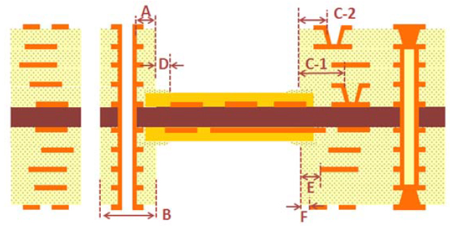
| Design Rules of Rigid-flex | |||||
|---|---|---|---|---|---|
 |
|||||
| Symbol | Description | Standard | Advanced | ||
| A | Through via hole edge to rigid/flex transition | ≥0.75 | ≥0.5 | ||
| B | NPTH edge to rigid/flex transition | ≥1.25 | ≥1.0 | ||
| C-1 | Laser via hole edge to rigid/flex transition(Laser to Flex Core) | ≥0.75 | ≥0.5 | ||
| C-2 | Laser via hole edge to rigid/flex transition | ≥0.4 | ≥0.3 | ||
| D | Resin flow of rigid/flex transition | ≤1.0 | ≤0.5 | ||
| E | I/L copper feature edge to rigid/flex transition | ≥0.5 | ≥0.3 | ||
| F | O/L copper feature edge to rigid/flex transition | ≥0.381 | ≥0.25 | ||